
搜索结果: 1-15 共查到“半导体技术 semiconductor”相关记录34条 . 查询时间(0.384 秒)
Academy of Mathematics and Systems Science, CAS Colloquia & Seminars:Introduction of Semiconductor Measuring Equipment Technology
半导体测量 设备技术 半导体
2023/4/21
本报告结合个人在半导体量测设备技术行业的工作经历,简要介绍半导体领域的技术,主要包括芯片制造工艺流程,光学量测技术OCD,器件几何建模,光学仿真算法RCWA和明暗场检测设备图像处理集群。

A model system created by stacking a pair of monolayer semiconductors is giving physicists a simpler way to study confounding quantum behavior, from heavy fermions to exotic quantum phase transitions.

On Aug. 9, President Joe Biden signed into law the CHIPS and Science Act, which invests $52 billion in domestic semiconductor manufacturing through tax credits, as well as supports STEM research and e...
Silicon is one of the most abundant elements on Earth, and in its pure form the material has become the foundation of much of modern technology, from solar cells to computer chips. But silicon’s prope...
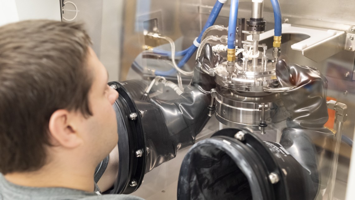
Cornell engineers and materials scientists have added a state-of-the-art tool to their suite of laboratory equipment that has helped make the university a world leader in the study of gallium oxide, a...

When it comes to creating next-generation electronics, two-dimensional semiconductors have a big edge. They’re faster, more powerful and more efficient. They’re also incredibly difficult to fabricate.
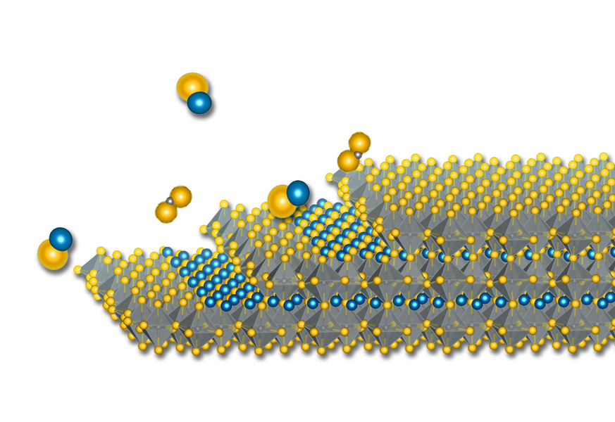
Engineers report a major advance in creating a new family of semiconductor materials(图)
半导体材料 硫族化 物钙钛矿 太阳能电池
2023/6/7
MIT engineers report creating the first high-quality thin films of a new family of semiconductor materials. The feat, which lead researcher Rafael Jaramillo refers to as his “white whale” because of h...
东南大学电子科学与工程学院研究团队在圆片级柔性InP半导体晶体管器件制备和封装技术方面取得重要进展,相关研究成果于近日被国际半导体行业著名杂志《Semiconductor Today》以《Flexible indium phosphide DHBT frequency boost》为题进行专题报道。柔性电子技术是目前电子行业所关注的重要研究方向,可广泛应用于电子通信、显示、太阳能电池、可穿戴设备、...

New ultrathin semiconductor materials exceed some of silicon’s ‘secret’ powers,Stanford engineers find(图)
New ultrathin semiconductor materials silicon secret powers Stanford engineers
2017/9/5
The next generation of feature-filled and energy-efficient electronics will require computer chips just a few atoms thick. For all its positive attributes, trusty silicon can’t take us to these ultrat...
2017年第二十八届SEMI先进半导体制造会议(2017 28th Annual SEMI Advanced Semiconductor Manufacturing Conference)(ASMC)
2017年 第二十八届 SEMI先进半导体制造 会议
2017/3/30
ASMC is the leading international technical conference for exploring solutions to improve the collective micro-electronics manufacturing expertise. The conference, with technical sponsorship from IEEE...
2017年能源应用半导体纳米线研讨会(Symposium NM7―Semiconductor Nanowires for Energy Applications)
2017年 能源应用半导体纳米线 研讨会
2017/3/9
Nanowires of a variety of materials (e.g., metals, group IV, III-V, II-VI semiconductors, oxides, chalcogenides, etc.) are promising building blocks for many existing and emerging applications. In par...
Graphene key to two-dimensional semiconductor with extraordinary properties
Graphene key two-dimensional semiconductor extraordinary properties
2016/9/12
A newly discovered method for making two-dimensional materials could lead to new and extraordinary properties, particularly in a class of materials called nitrides, say the Penn State materials scient...
The 23rd International Symposium on Room-Temperature Semiconductor Detectors (RTSD)
semiconductor radiation detectors imaging arrays
2016/7/21
The 23rd International Symposium on Room-Temperature Semiconductor Detectors (RTSD) represents the largest forum of scientists and engineers developing improved semiconductor radiation detectors and i...
UW scientists create ultrathin semiconductor heterostructures for new technological applications
UW scientists ultrathin semiconductor heterostructures new technological applications
2016/2/23
Heterostructures formed by different three-dimensional semiconductors form the foundation for modern electronic and photonic devices. Now, University of Washington scientists have successfully combine...
Team discovers way to 'tune' abundant elements for semiconductor use
Team tune abundant elements semiconductor
2015/11/12
In a world concerned about the dwindling supply and skyrocketing prices of rare elements used to make semiconductors, an international team of scientists and engineers has demonstrated that a new mate...